3D and Chiplet Integration Strategies for Advanced FPGA Architectures
Index
- Abstract
- Introduction
- Why FPGAs are Uniquely Suited
- Current Approaches for 2.5D and 3D FPGA Integration
- 2.5D Integration: Silicon Interposers
- 3D Integration: Die Stacking
- Fabrication and Packaging Challenges
- Future Directions and Optimization
- Conclusion
- References
Abstract
The rapid growth of computationally intensive fields such as artificial intelligence, edge computing, and computer vision had created a high demand for specialized computational chips such as Field-Programmable Gate Arrays (FPGAs). However, the traditional method of simply increasing the number of gates on a chip has become much more difficult. In a post-Moore era, where transistors can't become much smaller, there has been a push for creating larger monolithic chips. However, chips like these are often limited by die size, manufacturability, yield and power density, limiting their scalability. This report examines the shift from focusing on decreasing the size of a transistor to advanced packaging strategies as a solution. As identified by the SRC Microelectronics Roadmap, heterogeneous integration, 2.5D/3D packaging, and chiplet-based architectures are becoming increasingly important for extending device functionality. Specifically for FPGAs, these technologies offer ways for higher performance, improved yield, lower power and better thermal management. This report analyzes current 2.5D and 3D integration techniques, looks at fabrication and packaging challenges, and offers future directions, including hybrid bonding and chiplet optimization.
Introduction
We are in the "post-Moore" era, where traditional transistor scaling alone can no longer provide the desired gains in computing. This has driven a high demand for both larger, and more specialized chips. FPGAs have opportunities and use-cases in applications from data center acceleration to edge computing and AI. However, fabricating a single, large, complex FPGA die on a cutting edge process node faces limitations. As die size increases, manufacturing yield drops significantly, making large chips economically unviable [1]. This constraint limits the amount of compute, memory, and I/O that can be placed on a single die.
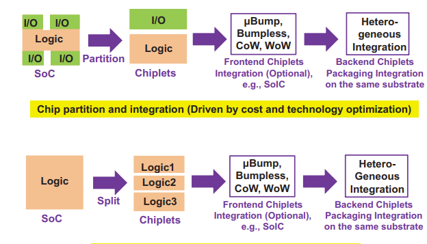
To overcome this challenge, the industry is turning towards advanced packaging. These strategies move away from the traditional System-on-Chip (SoC) model, where all functions are packed onto a single die, to a System-in-Package (SiP) model [1]. By separating the different functions of a larger design into smaller, distinct dies called chiplets, these functions can be fabricated separately, often using different process technologies, then integrated [1, 12].
Why FPGAs are Uniquely Suited
FPGAs were among the first use cases for 2.5D/3D integration for a couple reasons:
Monolithic Yield Collapse: The main way to add capacity to an FPGA is to make the die larger. In 2011, Xilinx (now AMD) had this exact problem, experiencing "very poor" yield when attempting to fabricate a large 28nm FPGA SoC [1]. 2.5D integration, specifically Xilinx's Stacked Silicon Interconnect (SSI) technology, solved this by connecting multiple smaller, high-yield FPGA "slices" onto an interposer to create a single, massive virtual FPGA [1, 5, 13].
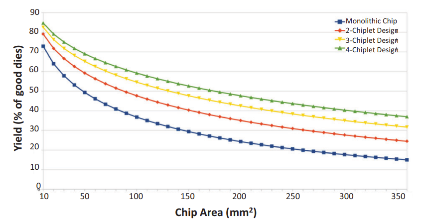 Chip area and yield of resulting chip for monolithic and multi chip designs
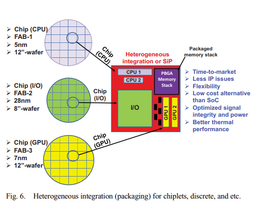
Ideal Case for Heterogeneous Integration: Modern FPGAs are incredibly complex SoCs that integrate multiple components, logic as FPGA fabric, CPU's, memory, and analog I/O [1]. Not all of these technologies require the same process nodes. Analog I/O for example benefits very little from expensive cutting edge process nodes [1]. Chiplets allow the core logic to be built on an expensive, cutting-edge process node while other parts of the chip like the I/O controllers remain on a mature, less costly process as seen in AMD's chiplet designs. Additionally, different substrate materials, such as GaN, can be used for the I/O controllers which may have high power applications [1].
High Bandwidth Memory Requirements: The AI and data-intensive workloads that FPGAs are used for often require massive memory bandwidth. 2.5D and 3D integration provides very short, high density interconnects, allowing high bandwidth memory to be placed directly beside or on top of the FPGA logic, greatly decreasing latency and power consumption compared to off-chip memory [1, 4, 12].
Current Approaches for 2.5D and 3D FPGA Integration
The move toward chiplet integration began as a solution to the yield and cost problems of large monolithic chips, with FPGA companies being early adopters [1, 5].
2.5D Integration: Silicon Interposers
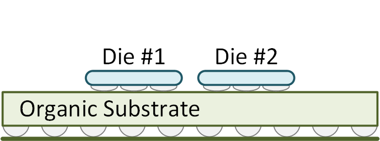
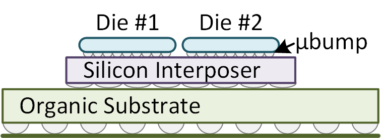
2.5D integration is the most established advanced packaging technique used in high-performance FPGAs. In this approach, chiplets are placed side-by-side on a silicon interposer which acts as a high-density wiring layer connecting between them.
Technology: The interposer connects dies using high-density microbumps, giving significantly more interconnect density and bandwidth than a traditional organic substrate [4].
FPGA Example: Xilinx's Stacked Silicon Interconnect technology, used in their Virtex series FPGAs, was a foundational commercial application of 2.5D integration [1, 13]. This allowed them to connect multiple FPGA "slices" on an interposer to create a single, massive FPGA that would have been impossible to build as one monolithic die [5, 13].
3D Integration: Die Stacking
3D integration turns the actual chips into interposers. Rather than placing chiplets side-by-side, they are stacked on top of each other. This approach allows for the shortest possible interconnect paths, promising significant gains in performance and power efficiency [2, 12].
Technology: Stacking is achieved using Through-Silicon Vias (TSVs), which are vertical electrical connections that pass through a silicon die [1]. Fabrication methods include Chip-on-Wafer (CoW) and Wafer-on-Wafer (WoW), which bond and integrate the stacked chiplets [1, 2].
Fabrication and Packaging Challenges
While 2.5D and 3D integration solve many problems, they have their own set of unique challenges in fabrication, packaging and design [2, 9].
Thermal Management
Heat is a large obstacle, especially for 3D stacking. While 2.5D can be used to better manage heat, stacking active dies on top of each other creates significant thermal density leading to "hotspots" that can decrease performance or damage the device.
Modeling: Accurate thermal analysis is essential. Research is ongoing into multi-fidelity thermal modeling frameworks that can quickly and accurately predict the thermal behavior of complex 2.5D and 3D systems [7].
Mitigation: One proposed methodology, TAP-2.5D, involves strategically inserting spacing between chiplets to minimize peak temperatures while co-optimizing for wirelength [6]. System-level cost analysis must also explicitly include thermal modeling to determine the most cost-effective and thermally-viable integration path [10].
Signal and Power Integrity (SI/PI)
The dense, high-bandwidth interconnects in 2.5D and 3D packages are highly susceptible to electrical noise, crosstalk, and voltage drop. Clean signals and stable power delivery are critical design considerations, especially for the high-speed interconnects needed for modern AI and ML infrastructure.
Design
Traditional 2D design tools are not designed to handle the complexities of 3D chips. New EDA tools are required to address [9]:
- 3D Floorplanning and Routing: Optimizing the placement and connection of chiplets in three dimensions.
- Electro-Thermal Simulation: Co-simulating the electrical and thermal properties of the entire package.
- Cost and Layout Modeling: Developing new frameworks to analyze the PPPA (Power, Performance, Price, and Area) trade-offs of different chiplet configurations [4].
Cost
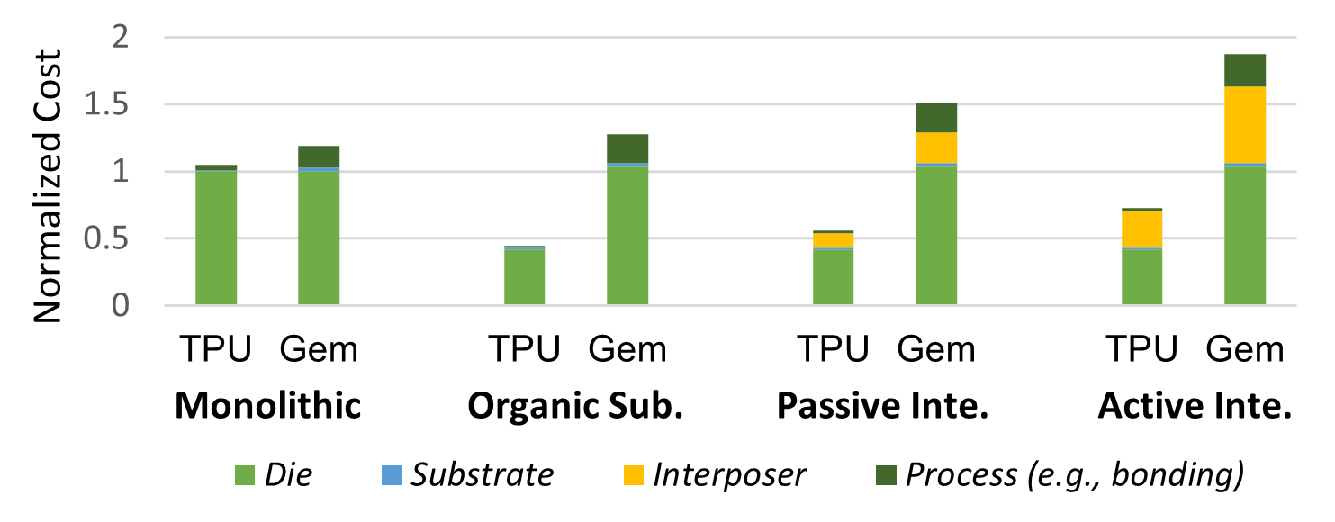
Advanced packaging is expensive. The fabrication of silicon interposers, etching TSVs, and complex bonding processes add significant cost. Analysis suggests that chiplet-based technology may only become cost-effective for larger, more complex chips [4]. Accurate cost modeling that includes die fabrication, bonding, and substrates is crucial for making design decisions. There is often a trade-off between the cost of the packaging, and the cost of the decreased yield from larger chips [4, 10].
Future Directions and Optimization
Modern chip research is focused on overcoming the aforementioned challenges and unlocking the next level of performance from chiplet-based systems.
Fine-Pitch Hybrid Bonding
A key future technology is fine-pitch hybrid bonding as a chip adhesion technique [1]. Unlike microbumps, which are small solder balls, hybrid bonding creates a direct copper connection between stacked dies at an incredibly small pitch.
This bumpless technology allows for dramatic increase in I/O density and bandwidth, creating a seamless connection between chiplets in both 3D and 2.5D integration. This is seen as a critical enabler for future high-performance 3D-ICs [1].
High-Bandwidth Interconnects
The performance of any chiplet system is ultimately limited by the interconnects. Future work is focused on:
- Latency Modeling: Using FPGA-accelerated simulation platforms like FireSim to productively and accurately model the latency of chiplet interconnects [8].
- Design for Integrity: Developing new interconnect designs that solve the signal integrity, power integrity, and electromigration challenges at extremely high bandwidths [11].
Chiplet Optimization
The future of chiplet design lies in customization and optimization for specific workloads [4, 12].
- Workload Specialization: FPGAs can be combined with chiplets designed for specific tasks, such as tensor workloads (e.g., matrix multiplication, convolution) common in AI [4].
- Specialized Networks: This includes designing specialized in-package networks (or "networks-on-chip") that are optimized to match the communication flow between these different chiplets [4].
- PPPA Optimization: The ultimate goal is to use modeling frameworks to optimize the entire system for its specific PPPA (Power, Performance, Price, and Area) targets [4].
Conclusion
As the benefits of traditional monolithic scaling diminish, 3D and chiplet integration strategies have become essential for the "post-Moore" era. FPGAs, given their inherent scalability challenges and heterogeneous nature, have been at the forefront of this shift, with Xilinx's 2.5D SSI technology serving as a foundational example [1, 5, 13].
While 2.5D integration is now a mature technology, the move toward true 3D stacking presents formidable challenges in thermal management, signal integrity, EDA tool design, and cost [2, 6, 9, 10]. Future progress for advanced FPGA architectures will be defined by innovations in these areas. The development of fine-pitch hybrid bonding [1], ultra-high-bandwidth interconnects [11], and workload-specialized chiplet ecosystems [4, 12] will be critical for realizing the next generation of high-performance, heterogeneously integrated FPGA systems.
References
[1] J. H. Lau, "State-of-the-Art and Outlooks of Chiplets, Heterogeneous Integration and Hybrid Bonding," Journal of Microelectronics and Electronic Packaging, vol. 18, no. 4, pp. 145–160, Dec. 2021.
[2] S. Singh and A. Kumar, "Challenges and Recent Prospectives of 3D Heterogeneous Integration," Materials Today: Proceedings, vol. 62, pp. 2532–2538, 2022.
[3] R. Sharma and P. K. Singh, "Emerging Chiplet-Based Architectures for Heterogeneous Integration," International Journal of Computer Science and Engineering Information Technology (CSEIT), vol. 5, no. 1, pp. 243–249, 2025.
[4] S. B. R. K. P. P. K. Tatikonda et al., "CHIMERA: A Framework for Cost-effective, Holistic, and In-depth Modeling of Chiplet-based Accelerators," arXiv preprint arXiv:2302.11256v3, 2023.
[5] S. J. L. L. S. T. S. et al., "2.5D TSV-Based Integration for High-Performance FPGA," in 2012 IEEE International Solid-State Circuits Conference Digest of Technical Papers (ISSCC), Feb. 2012, pp. 254–256.
[6] Y. Ma, S. S. Sapatnekar, and A. K. Joshi, "TAP-2.5D: Thermal-Aware Partitioning of 2.5D-IC," in 2021 Design, Automation & Test in Europe Conference & Exhibition (DATE), 2021, pp. 1018–1023.
[7] Z. Zhang et al., "A Multi-Fidelity Thermal Modeling Framework for 2.5D and 3D Integrated Circuits," arXiv preprint arXiv:2410.09188v2, 2024.
[8] D. J. Kim et al., "Productive and Accurate Latency Modeling of Chiplet Interconnects using FPGA-Accelerated Simulation," EECS Department, University of California, Berkeley, Tech. Rep. UCB/EECS-2022-145, 2022.
[9] Z. Zhou et al., "The Survey of Chiplet-based Integrated Architecture: An EDA Perspective," IEEE Access, vol. 11, pp. 28096–28124, 2023.
[10] I. A. E. G. O. et al., "System-level cost analysis with thermal modeling for 2.5D and 3D integration," in 2016 IEEE Computer Society Annual Symposium on VLSI (ISVLSI), 2016, pp. 244–249.
[11] S. K. S. et al., "High-Bandwidth Chiplet Interconnects for Advanced Packaging Technologies in AI/ML Applications: Challenges and Solutions," ResearchGate Preprint, Nov. 2024.
[12] R. Sharma and P. K. Singh, "Emerging Chiplet-Based Architectures for Heterogeneous Integration," ResearchGate Preprint, May 2024.
[13] D. Saban, "Xilinx Stacked Silicon Interconnect Technology Delivers Breakthrough FPGA Capacity, Bandwidth, and Power Efficiency," Xilinx White Paper, WP380 (v1.1.1), 2011.